Printed Circuit Boards (PCBs) are the backbone of a myriad of devices, serving as the critical link between component functionality and device reliability. The process of PCB design and fabrication is a sophisticated blend of engineering prowess and technological acumen, directly influencing the performance, durability, and cost-effectiveness of electronic products. As industries strive for innovation and efficiency, understanding the nuances of PCB design costs becomes paramount for manufacturers, engineers, and stakeholders alike.
This article aims to demystify the challenges of calculating PCB design costs, looking at the design process, fabrication intricacies, and the dynamic trends shaping the future of PCB manufacturing. By exploring the realm of PCB design services, circuit board design, and PCB board fabrication, we provide a comprehensive guide to cost calculation, ensuring informed decision-making in the competitive electronics market.
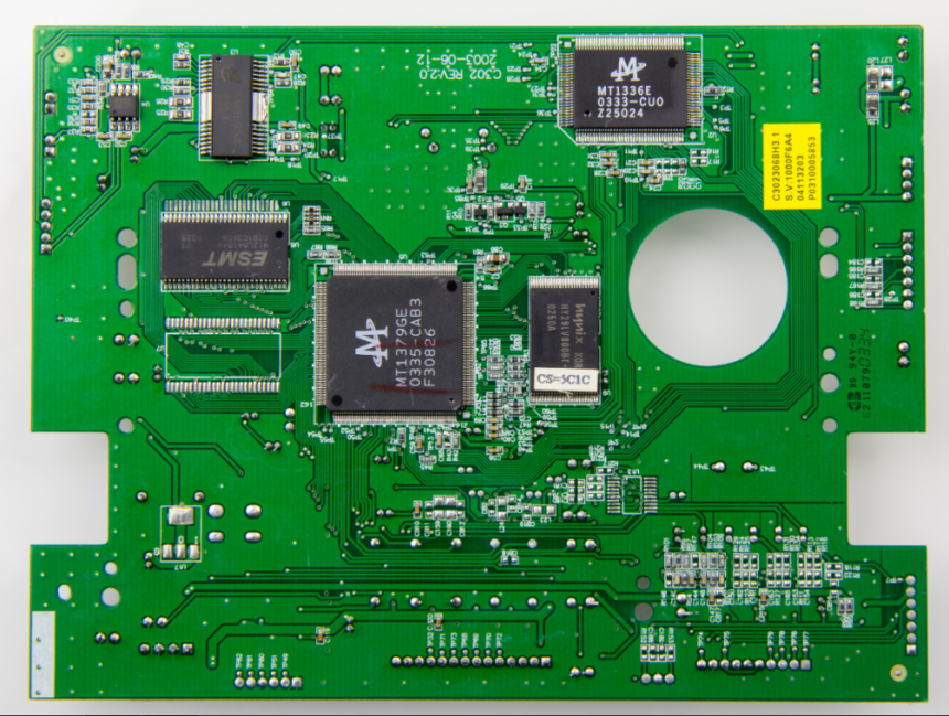
Understanding PCB Design and Fabrication
PCB design services play a pivotal role in the electronics manufacturing ecosystem, offering expertise that spans conceptual design to final product realization. These services encompass a broad spectrum of activities, including schematic capture, layout design, signal integrity analysis, and prototyping.
The essence of PCB design lies in its ability to translate electronic concepts into tangible, functional circuit boards that meet stringent performance and reliability standards. As such, the selection of a PCB design service is a critical decision, influenced by factors such as technical expertise, design efficiency, and cost-effectiveness.
The integration of advanced design methodologies and tools further enhances the value offered by these services, enabling the creation of complex, high-density PCBs that are fundamental to modern electronic devices.
Basics of PCB Board Fabrication
The fabrication of PCB boards is a complex, multi-step process that transforms a PCB design into a physical board capable of hosting electronic components. This process begins with the selection of a base material, typically FR4, which offers a balance of mechanical, thermal, and electrical properties suitable for a wide range of applications. Depending on the complexity and functionality required, PCBs can be single-sided, double-sided, or multilayer, each configuration offering distinct advantages in terms of circuit density and connectivity.
The fabrication process involves several key steps, including material preparation, pattern transfer, etching, drilling, and plating. Each step must be meticulously executed to ensure the integrity of the final product, with quality assurance measures in place to detect and address any defects. The choice of fabrication technology, such as traditional subtractive methods or advanced additive manufacturing, directly impacts the cost, precision, and scalability of PCB production.
One of the critical aspects of PCB board fabrication is the cost associated with each phase of the process. Material selection, for instance, significantly influences the overall cost, with high-performance materials commanding a premium.
Similarly, the complexity of the design dictates the number of fabrication steps required, directly affecting production costs. The decision between using standard technologies versus cutting-edge fabrication methods also plays a crucial role in determining the cost-efficiency of the manufacturing process.
The design and fabrication of PCBs are intricate processes that require a deep understanding of electronic principles, material science, and manufacturing technologies. The cost of PCB design and fabrication is influenced by a myriad of factors, from the complexity of the circuit and the materials used to the expertise of the design service and the chosen fabrication techniques.
As the electronics industry continues to advance, staying informed about the latest trends and innovations in PCB design and fabrication becomes essential for achieving cost-effective, high-performance electronic products. This article serves as a guide to navigating the complexities of PCB design costs, offering insights into the processes, challenges, and strategies that define the world of electronic manufacturing.
Factors Influencing PCB Design Costs
The calculation of PCB design costs is influenced by a constellation of factors, each contributing to the overall financial footprint of the design process. Understanding these factors is crucial for optimizing costs without compromising the quality or functionality of the final product.
Complexity and Size of the PCB
The complexity of a PCB design, often determined by the number of layers, the intricacy of the routing, and the density of components, significantly impacts design costs. More complex designs require advanced design skills, longer development times, and more sophisticated testing methodologies, all of which contribute to higher costs. Additionally, the physical size of the PCB plays a critical role; larger boards require more materials and are more challenging to design and test, further elevating the cost.
Material and Component Selection
The choice of materials for both the PCB substrate and the electronic components is a pivotal cost determinant. High-performance materials, such as high-frequency laminates or metal-core boards, are essential for certain applications but come at a premium. Similarly, the cost and availability of electronic components can fluctuate based on market demand, technological advancements, and supply chain dynamics, affecting the overall design cost.
Design Software and Tools
The selection of PCB design software and tools is another critical factor. Advanced design software packages, equipped with sophisticated simulation and analysis tools, can streamline the design process and reduce errors, but often require significant investment in licenses and training. Open-source or lower-cost alternatives may offer cost savings but might not provide the same level of functionality or support, potentially leading to longer design cycles or increased risk of design flaws.
Labor and Expertise
The expertise of the design team directly influences PCB design costs. Highly skilled designers and engineers command higher salaries but can navigate complex design challenges more efficiently, potentially reducing the time and resources required to bring a design to fruition. Balancing the cost of labor with the level of expertise required is a critical consideration for organizations seeking to manage design costs effectively.
The PCB Design Process and Cost Calculation
Understanding the PCB design process is essential for accurately calculating design costs. This process encompasses several stages, each with its own cost implications.
Step-by-Step Guide to the PCB Design Process
- Conceptualization and Schematic Design: This initial phase involves defining the electronic circuitry and creating a schematic diagram. Costs associated with this phase include labor for design engineers and the cost of any preliminary simulation software used to validate the concept.
- Layout Design and Simulation: During this phase, the schematic design is translated into a physical board layout, considering the optimal placement of components and routing of electrical connections. Advanced simulation tools are used to predict the performance of the PCB under various conditions, identifying potential issues before prototyping. The costs here include the labor of specialized layout designers and the software tools required for simulation and layout.
- Prototyping and Testing: Once the layout is finalized, prototype boards are manufactured and subjected to rigorous testing. This phase is crucial for identifying any design flaws or performance issues. Costs include prototype fabrication, testing equipment, and labor for testing and analysis.
Calculating Design Costs
To calculate the design costs accurately, it is necessary to consider both fixed and variable expenses associated with each stage of the design process. Fixed costs, such as software licenses and basic design tools, are relatively stable, while variable costs, such as labor and prototype fabrication, can fluctuate based on the complexity of the project and the number of iterations required to achieve a final design.
Effective cost calculation also involves anticipating potential revisions and incorporating contingency budgets to address unforeseen challenges. By understanding the cost drivers at each stage of the design process and adopting a strategic approach to resource allocation, organizations can optimize PCB design costs, ensuring a balance between cost efficiency and design quality.
PCB Board Fabrication Costs
The transition from PCB design to physical board fabrication introduces a new set of cost considerations, each pivotal to the overall budget of electronic product manufacturing. Understanding these costs is essential for businesses aiming to optimize their production strategies without sacrificing quality or functionality.
Pre-production Expenses
Before the actual manufacturing process begins, pre-production costs must be taken into account. This includes the expenses related to setting up manufacturing lines, creating the necessary tooling for new PCB designs, and preparing the fabrication plant for a specific production run. Tooling, in particular, can be a significant cost, especially for complex PCB designs requiring unique fixtures or custom drill bits.
Additionally, the cost of generating Gerber files, which are used to guide the fabrication process, falls into this category. These initial investments are crucial for ensuring a smooth and efficient manufacturing process, but they add to the overall cost of PCB fabrication.
Production Costs
Once pre-production is complete, the actual fabrication costs come into play. These costs are influenced by the volume of the production run, with larger quantities generally benefiting from economies of scale. However, the complexity of the PCB design also plays a crucial role; more complex boards require more time-consuming processes such as intricate etching and multiple layers of lamination, which can increase costs.
Material choices also impact production costs, with high-end materials like high-frequency laminates or flexible substrates commanding higher prices. Additionally, the method of PCB assembly—whether surface mount technology (SMT), through-hole technology (THT), or a combination of both—affects the overall fabrication cost, with SMT generally being more cost-efficient for high-volume production.
Quality Assurance and Testing
Quality assurance (QA) and testing are integral parts of the PCB fabrication process, designed to ensure that the final products meet the required specifications and are free from defects. This phase can involve a variety of tests, such as in-circuit testing, functional testing, and environmental stress testing, each adding to the cost of production.
However, investing in thorough QA and testing can ultimately save money by reducing the rate of product failures and returns, highlighting the balance between upfront costs and long-term savings.
Trends Affecting PCB Design and Fabrication Costs
The PCB industry is subject to continuous evolution, with new technologies, manufacturing techniques, and market dynamics shaping the cost landscape. Keeping abreast of these trends is crucial for companies looking to stay competitive and cost-efficient.
Technological Advances
Recent years have seen significant technological advances in PCB design and fabrication, such as the rise of flexible PCBs, the adoption of HDI (High-Density Interconnect) technology, and the increasing use of 3D printing for prototyping and even production. These innovations can lead to higher initial costs due to the need for specialized equipment and materials.
However, they also offer the potential for long-term savings and competitive advantages, such as reduced material usage, lower shipping weights, and the ability to design more compact and efficient electronic devices.
Global Supply Chain and Market Trends
The global nature of the electronics supply chain introduces variability in the costs of raw materials and components, influenced by geopolitical events, trade policies, and fluctuations in demand. For instance, tariffs on imported materials can increase costs, while shortages of critical components, as seen in recent years, can lead to production delays and increased prices.
Companies must navigate these challenges by diversifying their supply chains, investing in inventory management, and closely monitoring market trends to mitigate risks and manage costs effectively.
Sustainability and Environmental Regulations
Sustainability and compliance with environmental regulations are becoming increasingly important in the PCB industry. Regulations such as the Restriction of Hazardous Substances (RoHS) and the Waste Electrical and Electronic Equipment (WEEE) Directive impose requirements on the use of certain materials and the recycling of electronic waste.
While adhering to these regulations can increase production costs due to the need for alternative materials and compliance testing, it also opens up opportunities for companies to differentiate themselves in the market by offering environmentally friendly products.
Cost Optimization Strategies
In the intricate world of PCB design and fabrication, cost optimization plays a pivotal role in maintaining competitiveness and ensuring profitability. Implementing strategic measures to reduce costs without compromising on quality is essential for businesses aiming to thrive in the dynamic electronics market.
Design for Manufacturability (DFM)
Design for Manufacturability (DFM) is a proactive approach to PCB design that focuses on simplifying the manufacturing process and reducing production costs. By considering manufacturing constraints and challenges during the design phase, companies can avoid costly design revisions and fabrication errors.
DFM principles include optimizing the layout for easier assembly, selecting standard components to reduce costs, and ensuring that the design complies with industry standards to avoid custom fabrication processes. Embracing DFM can lead to significant savings in both time and resources, enhancing the overall efficiency of the PCB production cycle.
Choosing the Right PCB Design Services
Selecting the appropriate PCB design services is crucial for cost optimization. Companies should look for service providers that offer a balance between quality, expertise, and cost-effectiveness. This involves evaluating the provider’s track record, technological capabilities, and understanding of industry-specific requirements.
Additionally, transparency in pricing and the ability to offer scalable solutions as per project demands can be determining factors. By partnering with a reliable PCB design service, companies can leverage expert knowledge and advanced tools to optimize design processes, reducing costs in the long run.
Long-term Partnerships and Negotiations
Establishing long-term partnerships with suppliers and service providers can lead to cost benefits through negotiated rates, priority service, and improved supply chain reliability. Companies that develop strong relationships with their vendors can often secure better prices for materials and services, thanks to the volume of business or the mutual interest in maintaining a steady partnership. Furthermore, these relationships can facilitate faster response times and more flexible terms, which are invaluable in managing the fast-paced demands of the electronics industry.
Conclusion
The journey from PCB design conception to fabrication is fraught with cost implications at every turn. Understanding these costs—stemming from design complexity, material selection, labor, and technological advancements—is paramount for businesses striving to maintain a balance between affordability, quality, and innovation.
By adopting cost optimization strategies such as DFM, judiciously selecting design services, and fostering long-term partnerships, companies can navigate the cost landscape more effectively. As the electronics industry continues to evolve, staying informed and adaptable will be key to achieving cost-efficient PCB design and fabrication.
This article has provided a comprehensive overview of the factors affecting Hdi PCB design costs and outlined strategies to optimize these costs, offering valuable insights for businesses looking to enhance their competitive edge in the global electronics market.