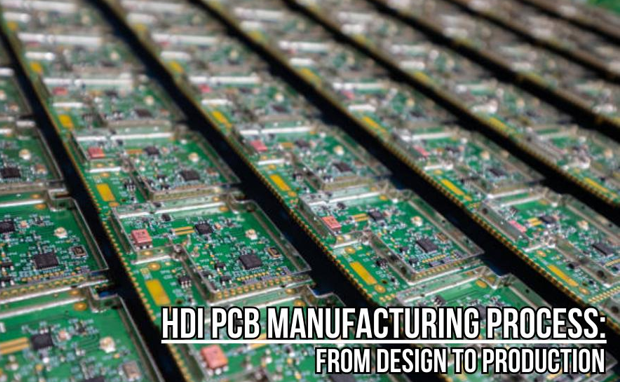
Technology is constantly marching, and the demand for compact but powerful printed circuit boards is on the rise. One of the potential solutions to this issue is high-density interconnect techniques, which will contribute to miniaturizing PCBs and turning them into compact powerhouses that can be integrated into a multitude of devices.
In this article, we’ll be discussing the HDI PCB manufacturing process, which will entail the steps from design to the manufacturing phase.
What’s an HDI PCB?
To begin our discussion, let’s understand what a high-density interconnect printed circuit board is. HDI PCB boards are characterized by their high wiring density per unit area when you compare them to standard printed circuit boards. These PCBs are also best summed up as a supercharged version of conventional electronic boards, which allows them to be manufactured in smaller sizes.
However, don’t let the small size fool you; an HDI board is more than capable of integrating into different devices with ease, which makes them an appealing addition to many electronics in varying niches.
The HDI PCB Designing Phase
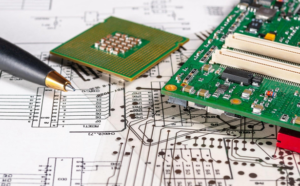
Before we explore the steps in successfully fabricating a high-density interconnect PCB, we’ll have to discuss the steps in designing an HDI PCB. Without a proper design, you won’t be able to come up with functional and practical printed circuit boards that can be utilized by different electronics. Here are the steps that encompass the design phase for HDI circuit boards.
1. Creating a schematic
The first step is to create a schematic diagram of the HDI PCB board. This schematic is a representation of all the components utilized in the printed circuit boards, along with their linkages. The diagram also shows the layout of all electrical connections present on the PCB, and this includes linkages found between the components, circuits, and the system it is going to be linked to.
2. Drafting a layout of the board
Once you are done completing the schematic for the HDI PCB board, you will need to start making the layout drawing. The layout drawing will show where all of the components and parts will be positioned on the high-density interconnect printed circuit board. This layout that you are drawing should be created through the use of a computer-assisted milling application.
3. Forwarding the layout to a manufacturer
If you are happy with the layout that you’ve drawn through the use of a computer-assisted milling tool, submit it to your partnered HDI PCB manufacturer. Your manufacturer will then receive the files from your end and run a few checks to see whether the design is practical to make. If not, you’ll have to apply some revisions and changes to the design and submit it to your partner manufacturer.
If your manufacturer deems the HDI board’s design as practical to make, they have the design files converted to a file format that their reading machines can perceive. At this point, the designing phase of the process ends and the manufacturing half begins.
The HDI PCB Manufacturing Phase
The manufacturing half of making an HDI PCB board begins at the moment that your manufacturer transmits the approved PCB design to their work machinery. The manufacturing process takes place mostly on the assembly line, where the components and parts undergo multiple steps before being assembled and given multiple tests for quality assurance.
Here are the steps that entail the manufacturing half of making a high-density interconnect printed circuit board.
1. Manufacturing of HDI PCB bare board
When the HDI PCB design is finished, it is time to produce the PCB bare board. HDI circuit board is one of the most high-tech PCBs, so very experienced and reliable PCB manufacturers are needed to produce DHI PCBs. Please note that HDI PCB manufacturing always needs a longer lead time, it is normal to wait 4-6 weeks to get them done.
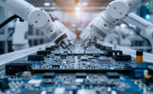
2. Installing the components
The next step in manufacturing and assembly of an HDI PCB board consists of two parts: one is applying the solder and the other is installing the components. This step is kicked off by the PCB assembly manufacturer transmitting the received files to the factory’s pick-and-place machines to automate the placement of essential parts on the board.
Once solder paste printing is done, the blank boards are sent in on the assembly line, where they will pass through the pick-and-place machines, adding and installing parts as they proceed along the assembly line.
3. Reflow soldering for SMD components
Now that the SMD parts of the HDI PCB board are in position, the next step involves the component-studded boards passing along the soldering section of the assembly line, that is reflow soldering. This reflow soldering equipment will heat and melt the solder that will be used to keep the components intact and prevent them from falling off the PCBs.
Once the linkages are in place, the PCBs undergo a baking process in an industrial oven. The boards are exposed to high temperatures for several minutes, wherein it is hot enough to melt the solder paste to fully cement the components and connectors in their final positions.
The process of soldering will keep for a few minutes since there are 8-12 temperature zones, to make sure all the components on the printed circuit board will be soldered in good condition.
4. PTH assembly and Final assembly
The penultimate steps in assembling a high-density interconnect circuit board involve the PTH components assembly and final assembly of the PCBs. In the PTH assembly process, the PCB boards are then fitted with PTH components such as connectors that allow them to link up with input or output devices such as buttons or switches.
During the final assembly, the PCBs are going to be assembled so that they will exhibit their finished appearance.
- Test runs for functionality
The final step in manufacturing an HDI PCB encompasses multiple trial runs or tests conducted on the printed circuit board. The finished boards are tested on various equipment, ranging from oscilloscopes to spectrum analyzers, to check if the traces are working as intended. The finished boards are also checked with devices such as the optical inspection tool to detect any post-manufacturing defects.
Should there be any defects, the boards are subjected to either quick repairs where the defective parts are fixed and tested again, or remanufacturing, which involves disassembling, repairing, replacing, re-assembly, and conducting another round of tests.
A straightforward process for a powerful circuit board
Now that you’ve learned the ins and outs of the process of HDI PCB manufacturing, you will soon realize how much care is put into the production of these technological powerhouses. After all, the goal of your partnered HDI PCB manufacturer is to provide you with functioning HDI boards so that they can be integrated into the tools of your business or your store’s electronic merchandise.
Not only you will reap the benefits of utilizing these powerful circuit boards but your customers too as they use their gadgets with little to no problem.